With the rapid development of LED display technology, recently, SMD(Surface Mounted Devices) packaging products are not not satisfactory but solutions for LED screens. And for this reason, more and more cutting-edge packaging technologies in the LED display market are welcomed by the mid-to-high-end display market and become a new trend for future displays.
Following I will introduce to you 3 kinds of packaging technology of LED lamps (COB, AOB and GOB technology), including their functions, working methods and applications.
Evolution of LED Encapsulation Technology
When it comes to LED packaging technology, we all know SMD which came into being about 20 years ago. From passive components to active components and integrated circuits, eventually became surface mount devices (SMD) and can be assembled by mounter equipment. Now new technologies have emerged in the market that can greatly improve the stability, reliability and individuality of the LED screens.
Definition of COB, AOB and GOB
COB is the abbreviation for Chip On Board, and AOB for Admixture On Board, GOB for Glue On Board. They are all innovative packaging technology in the LED lamps.
Chip-on-Board or "COB" refers to the mounting of a bare LED chip in direct contact with a substrate or PCB board to arrange LED beads. Compared with traditional LED packaging technology, like surface mount device ("SMD") LED or dual in-line package ("DIP") LED, COB LED has many advantages, because it can achieve higher packing density of the LED array.
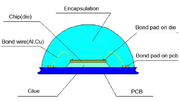
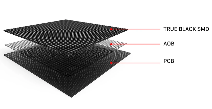
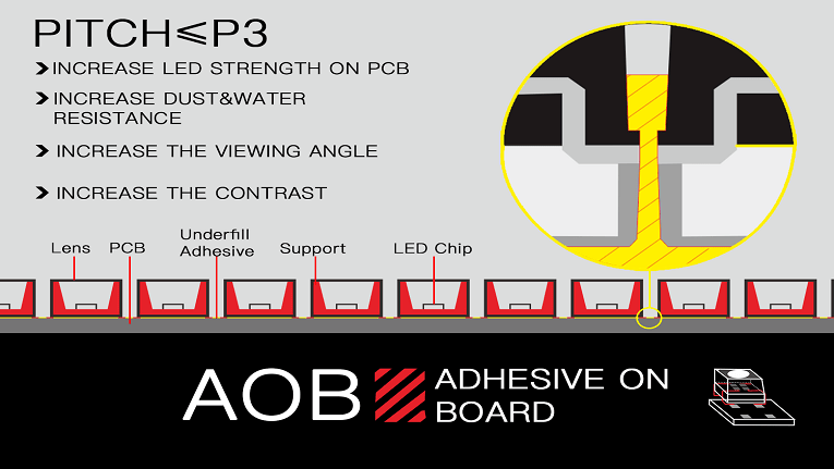
AOB is another encapsulation technology that increases the strength of the LED bead on the PCB, enhances the performance of waterproof and dustproof of the screen, expand the viewing angle of the screen and enhances color contrast of the visual effect.
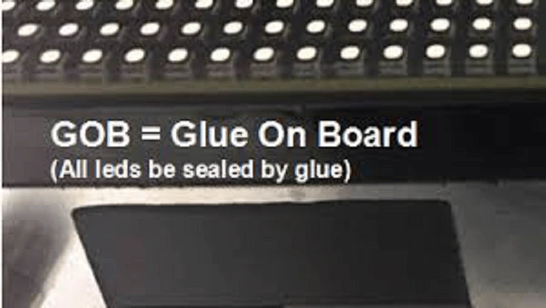
While GOB Technology is an innovative sealing on module surface with an epoxy Glue. It is a great protection of the LED on the LED modules from Water, dust and damage.
According to the definition, we know that in the process of installing and using SMD screens, the role of COB and GOB packaging technology is basically to protect LED lights from damage caused by knocking and scratching and the scraping of lamp board, while COB technology is mainly used in small pixel pitch LED screen to increase the density of the LED beads, so that we can get a high-density led beads screens.
How do they work to improve the performance of LED screens?
As mentioned above, COB technology allows for a much higher packing density of the LED array. So with COB LED technology, more LED beads can be mounted in a limited area, the color of the picture is richer, and the visual effect of the screen is more beautiful. Take an instance, on a 10mm x 10mm square array, COB technology will result in 38 times more LEDs compared to DIP LED technology and 8.5 times more LEDs compared to SMD LED technology (see diagram below).
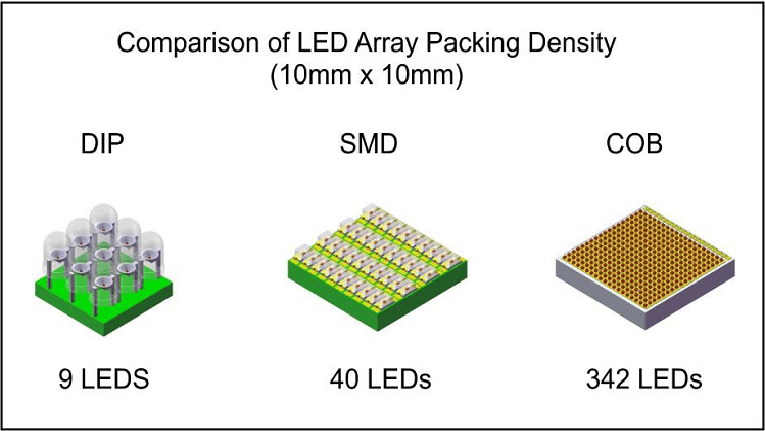
This leads to higher intensity and greater uniformity of light. Alternatively, the use of COB LED technology can greatly reduce the footprint and energy consumption of the LED array while keeping light output constant. For example, a 500 lumen COB LED array can be many times smaller and consume substantially less energy than a 500 lumen SMD or DIP LED Array.
Another major advantage of using COB LED technology lies in the fact that COB devices have only 1 circuit and 2 contacts for the entire chip. Regardless of the number of diodes, this single circuit design can simplify the work of other LED devices.
The advantages of Chip-on-Board LED arrays include:
1)Compactness due to the small size of the chip.
2)High-Intensity, particularly at close distances.
3)High-Uniformity, even at close working distances.
4)Design Simplicity because only 1 circuit and 2 contacts are required.
5)Superior Thermal Performance for increased life, stability and reliability.
So how does AOB technology work?
AOB (Admixture On Board) is the last process in the production of surface mount LED displays. After the SMT process is completed, a layer of silicon glue is coated on the surface of the light board, so during the installation work, the connection between the LED light and the PCB board achieves the purpose of anti-collision.
Before this process, SMD screen has gone through the white balance of the lamp board for 72h, constant temperature aging and the 24h video aging of the whole screen. Excluding the various defects caused by the production process and components, the isolation protection by AOB nano-coating will reduce the LED failure rate to below 5PPM, which greatly improves the yield and reliability of the screen.
And how does GOB technology work?
GOB Technology is an innovative sealing on module surface with an epoxy film. It is a great protection of the LED on the LED modules from water, dust and damage. Different from AOB technology, GOB technology protects the screen by isolating the LED lamp from water, dust and collision, so that the led lamps won’t be broken and work properly even with water and dust whereas AOB technology prevents the screen from damage by strengthening the connection between LED beads with PCB board.
How can we apply COB, AOB and GOB technology to the screen?
All three of them are all used in small pitch led screens whose pixel pitch is narrower than P3. And the protection rate decrease with hierarchical order: AOB - GOB - COB. For screens within P2-P3 range, we suggest AOB technology and for outdoor rental LED screens with pixel pitch narrower than P2, we suggest GOB and for small pitch led screens, it would be better to choose COB.
By continuing to use the site you agree to our privacy policy Terms and Conditions.