Fine Pitch LED Display: A Complete Guide to Sizes, Advancements & Packaging
Views: 6357
Author: Site Editor
Publish Time: 2024-11-29
Origin: Site
The rapid evolution of LED technology has positioned fine pitch LED displays as the premier solution for high-end indoor visualization needs. Characterized by their seamless splicing capability, exceptional color accuracy, and energy efficiency, these displays now dominate mission-critical environments ranging from command centers to corporate boardrooms.
Understanding Fine Pitch LED Technology
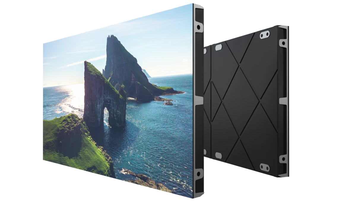
At its core, a fine pitch LED display refers to any LED panel with pixel spacing below 2.5mm, typically ranging from 1.0mm to 2.5mm. This tight pixel density enables viewers to experience crisp imagery even at close distances, fundamentally differentiating it from conventional LED signage. The technology achieves this through advanced surface-mount device (SMD) packaging where individual RGB LEDs are mounted directly onto PCBs with sub-millimeter precision.
What truly sets fine pitch LED apart is its combination of performance characteristics. These displays maintain perfect black levels at brightness as low as 300 nits while delivering 16-bit grayscale performance, making them ideal for prolonged viewing in control rooms. Their 3840Hz+ refresh rates eliminate flickering during camera capture, a critical feature for broadcast studios. Perhaps most importantly, the complete absence of physical bezels allows for flawless multi-panel configurations - a decisive advantage over LCD or DLP video walls.
Industry Applications of Fine Pitch Led Display
The military sector was among the first to recognize fine pitch LED's strategic value. Command centers now employ these displays for their ability to present uninterrupted situational awareness maps across massive video walls. Air traffic control towers benefit from their sunlight-readable brightness and 180° viewing angles.
Corporate environments have followed suit. Fortune 500 companies increasingly install fine pitch LED video walls in executive briefing centers, where their true 4K resolution showcases detailed financial models and global supply chain visualizations. High-end retail spaces leverage the technology's vibrant colors and slim profiles to create immersive brand experiences.
Technical Considerations for Implementation
Implementing fine pitch LED solutions requires careful evaluation of several factors. Pixel pitch selection depends on viewing distance - the rule of thumb suggests 1mm pitch per meter of viewing distance. Thermal management becomes critical at pitches below 1.5mm, where advanced copper core PCB designs help dissipate heat from densely packed LEDs.
Calibration processes separate professional-grade installations from consumer products. Factory-level brightness and chromaticity calibration ensures color uniformity across every panel, while field-serviceable modules allow for quick maintenance without full system downtime.
The Road Ahead
While current fine pitch LED technology already outperforms alternative solutions, ongoing innovations promise further improvements. Emerging chip-on-board (COB) packaging techniques are pushing pixel pitches below 0.9mm while improving reliability. Meanwhile, advancements in driver IC technology enable higher refresh rates and lower power consumption.
As manufacturing costs continue to decline, industry analysts predict fine pitch LED will capture over 35% of the professional display market by 2026, particularly in sectors where image fidelity and reliability outweigh cost considerations. The technology's ability to scale from compact conference room installations to stadium-sized video walls ensures its position as the display solution of choice for the most demanding visualization challenges.